 |
Scottish
Centre for Interdisciplinary Surface Spectroscopy |
 |
|---|
The facilities available at SCISS
|
Angle
Resolved Photoemission Spectroscopy (ARPES)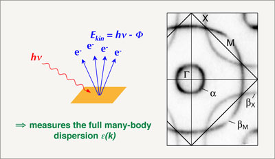 Angular resolved photoemission (ARPES) is a uniquely powerful tool for probing electronic quasiparticles. It is virtually the only spectroscopy with direct momentum resolution, a key advantage for the study of anisotropic and low-dimensional materials. ARPES data contain the band structure of a material, and, because the signal is proportional to the single particle spectral function, give detailed information on the propagation of electrons in the full many-body system. ARPES characteristics He Iα (21.2 ev) and He IIα (40.8 eV) rotable linear polarization (> 80%) energy resolution Δε = 3 ÷ 10 meV routinely ± 13° parallel recording spot size: 0.5 mm2 automated k-space mapping XPS characteristics Al Kα(1486.6 eV) monochromatized (Δε < 300 meV) Sample environment ultra-high vacuum (< 5 x 10-11 mbar) 6 - 450 K 6 degrees of freedom (3 rotations, 3 translations) Surface preparation automated sputter/anneal (< 1400 K) low-energy electron diffraction (LEED) evaporators, thickness monitor evaporation on < 10 K substrates in "upper chamber" System setup 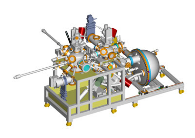 SPECS instrument, delivered in June 2008 |
Scanning
Tunnelling Microscopy/Spectroscopy (STM/STS)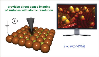 Scanning probe microscopies (STM and AFM) are the most exquisite tools to not only investigating the geometric, but also the electronic structure of flat surfaces at the atomic scale. When operated at low temperatures, one can uniquely benefit of electronic spectroscopy (STS) and vibrational spectroscopy (IETS) at the single atom/molecule level. Furthermore, atomic manipulations allow for a tailored design of nano-structures. STM, AFM and their spectroscopy modes have revolutionized our understanding of the physics and chemistry at surfaces. STM/STS characteristics base temperature 5 K scan range 1 µm at 6 K, 1.5 µm at 77 K max drift rate at 6 K: < 0.2 nm/hour residual vibration level: < 2 pm easy switch STM/AFM system rests on a 14 tonnes concrete block for vibration isolation. Sample environment ultra-high vacuum (< 5 x 10-11 mbar) 4 degrees of freedom (1 rotations, 3 translations) Surface preparation automated sputter/anneal (< 1400 K) metal and molecular evaporators, thickness monitor LHe-cooled manipulator (20 - 1400 K) low temperature sample transfer to STM cleaver for special oxides low-energy electron diffrection and Auger spectroscopy (LEED/AES) System setup  CreaTec instrument, delivered in July 2008 |
Last update: 06/08/2014 - University of St Andrews